A (not so big) Primer on GPU Internals
Introduction
For the past couple of weeks, I’ve been exploring things that would be exciting to learn, be it how to structure workflows with different agentic harnesses, a couple of math stuff with classical MLs and quite a bit of other stuff, but I still didn’t find something that I would love to dive into, until I stumbled across CUDA kernels and Physics Of Inference in LLMs, I’ve been reading blogs, books, and quite a lot of chats with LLMs to help me understand all of this stuff and its just captivating.
For readers not familiar with CUDA kernels and Inference in LLMs, a kernel is a small program that runs on the GPU, and modern AI models like ChatGPT rely on thousands of these running in parallel to process your prompts (inference). Understanding the hardware they run on is key to understanding why some models are faster or cheaper than others.
GPU
There’s a lot of components that make up your PC, like CPU, Motherboard, but the one that is going to be the focus of this blog is GPU, which is quite literally the backbone of almost all the AI applications that you’re using nowadays
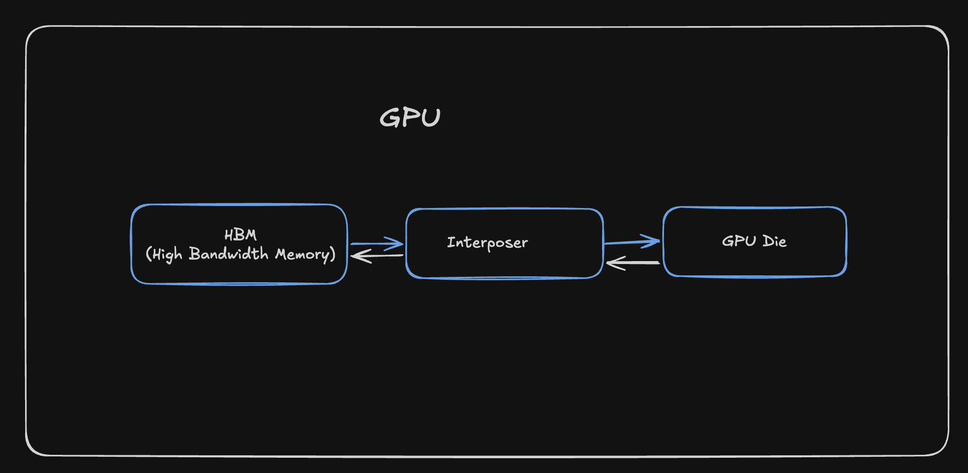
The GPU consists of 3 main parts
- HBM (High Bandwidth Memory)
- Interposer
- GPU Die
Before we get more into these components, we have to understand the different types of RAM that are used up in making these components
DRAM (Dynamic RAM)
These are the memory chips that are made up of a Capacitor and a Transistor. A transistor acts as a switch that controls whether charge can flow into or out of the capacitor, with a charged state representing 1 and an empty state representing 0. But due to the nature of a Capacitor leaking its charge, the DRAM has to constantly refresh the Capacitor to allow the same state to be persisted, this constant refreshing leads to slow memory transfers. One transistor and one capacitor per bit means you can pack a lot of memory into a small area, so they are dense and cheap(er).
SRAM (Static RAM)
These are the memory chips that are made up of a Flip Flop, which is made up of 6 Transistors, these transistors are used to store the state of the memory. They don’t require constant refreshing and hence are much faster. But due to the nature of the Flip Flop, they are also much more expensive. They are rather less dense and take up more space per bit of information.
HBM (High Bandwidth Memory)
HBM is a vertical stack of DRAM chips, This allows for very high bandwidth memory transfers, but at the cost of being more expensive and less dense.
Interposer
The interposer is a thin substrate that sits between HBM and GPU Die, it provides dense wiring so the GPU and the HBM can exchange data at high bandwidth with short electrical paths
GPU Die
This is by far the most important aspect of the entire GPU, anything that is kernel related or related to improving the overall performance of a program is directly impacted by the components present in the GPU Die
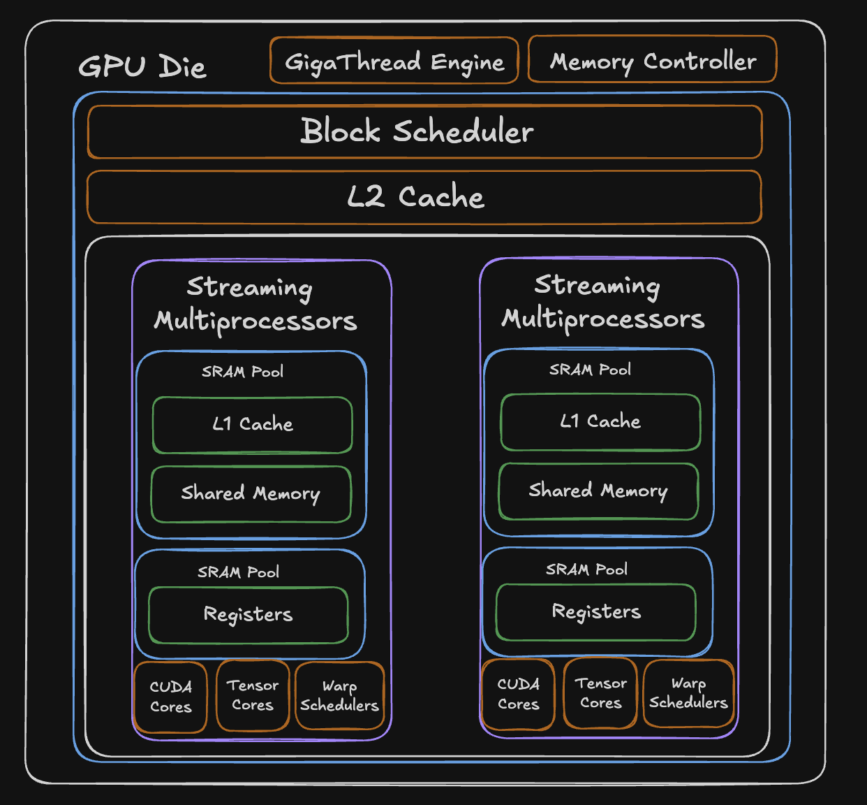
SMs (Streaming Multiprocessors)
A GPU die is made of many Streaming Multiprocessors (SMs). Each SM can run many threads in parallel, the work you launch from a kernel. A typical GPU has many SMs; each SM includes the following:
- CUDA Cores
- Tensor Cores
- L1 Cache
- Shared Memory
- Registers
These components are SRAM-heavy so they stay fast and close to the logical cores. On many NVIDIA-style GPUs, L1 and shared memory share the same on-chip SRAM, often with a configurable split between how much goes to L1 versus shared memory. Registers are separate: each SM has its own register file for the threads scheduled on it.
Apart from this, the die also contains memory controllers that are responsible for managing the memory traffic between the GPU and the HBM.
Now let’s look into the most important components in the die, the memory and logical units.
Memory Hierarchy
L2 Cache
The L2 cache is a large SRAM pool that sits at the die level, shared across all SMs. When an SM needs data that isn’t in its local L1 or shared memory, the request hits L2 before going all the way out to HBM. Because it’s on-die SRAM, it’s significantly faster than HBM while being larger than any individual SMs local memory.
Shared Memory
This is a programmer controlled memory that lives inside each SM. Unlike normal caches, shared memory doesn’t automatically decide what to store, you decide explicitly what data is to be loaded into it and read from it. This makes it useful when you know exactly what data you’ll need repeatedly. It shares a physical SRAM pool with the L1 cache, and the split between them is configurable.
This is very important when it comes to individual kernel performance, I will write more about this in the next blog, where I talk about how software is structured around GPU hardware.
L1 Cache
A hardware-managed cache inside each SM that shares the same physical SRAM pool as shared memory. Unlike shared memory, user doesn’t decide what goes in L1, the hardware automatically caches recently accessed data. It’s transparent to the programmer, acting as an automatic buffer between the SM and the slower L2/HBM.
Register Pool
The fastest memory on the entire GPU. Each SM has a dedicated SRAM pool of registers, 65,536 32-bit registers, meaning each register can hold 4 bytes of data. These are private to individual threads and hold the immediate values a thread is actively computing with. Access is essentially instant, but the pool is finite, so the more registers each thread uses, the fewer threads can run on that SM simultaneously.
Logical Units
CUDA Cores
The general-purpose arithmetic units inside each SM. Each CUDA core can perform one floating-point or integer operation per clock cycle,adds, multiplies, comparisons, and so on. An SM contains many of them, and they handle the bulk of non-matrix computation.
Kind of like any scalar mathematical operations that you do, they’re all handled by the CUDA cores.
Tensor Cores
Specialized hardware designed specifically for matrix multiply-and-accumulate operations. While a CUDA core does one operation per cycle, a tensor core can process an entire small matrix multiplication (like 4x4 or 16x16) in a single operation, so more compute happening in the same clock cycle. This is what makes modern GPUs so fast for AI workloads
Schedulers
Ideally, I would want to explain what schedulers do in granular details, but for the scope of this blog, I will abstract out the software complexities like warps, threads, blocks and grids, as they require a whole blog on their own.
GigaThread Engine
A dedicated hardware unit at the die level that distributes work across all SMs. It monitors which SMs have available resources and dispatches new tasks to them as capacity frees up.
Warp Scheduler
Each SM contains multiple warp schedulers that decide which group of threads (programs) gets to execute each clock cycle. When one group stalls waiting on memory, the scheduler instantly switches to another ready group with zero overhead, it’s still a bit complex to understand, but hopefully this gives a preface to what schedulers do.
Wrapping Up
I’ve been enjoying reading more about GPUs and their internals, never thought I would be dissecting the hardware internals of a GPU, but well, here we are. I’ll have another blog coming up soon that connects to the software side of GPUs and how it all fits together. In the coming months, I’ll be exploring more into the kernels and Reinforcement Learning stuff, so stay tuned for that.